Understanding the Unisoc BROM Protocol
This blog post will explore the Unisoc BROM protocol (Download Mode) used to flash firmware on devices running on unisoc chipsets. BROM mode is a universal low-level pre-boot state that is mostly used to program or write firmware on a device by the OEM.
The BROM Mode is present on different devices running on different chipsets but the communication protocol differs with each chipset. For example — consider the following known chipsets and their respective protocols:
- Mediatek: This chipset’s BROM implements a simple protocol that is compatible with a Download Agent (DA) – there is no known name for this protocol.
- Qualcomm: This chipset’s BROM implements the Firehose and Sahara Protocol 1
What is this BROM protocol?
When writing firmware to an android device — for this case a device running on the unisoc chipset — the device will first be booted to BROM. This can be done via the devices button combination for example (vol+/vol-) or via shorting a test-point on the device’s PCB.
A flashing tool for example — SPD Flash Tool 2 connected to the device via USB will then talk to the boot ROM 3 via Unisoc’s BROM protocol to write the firmware files to the device. These files include kernel and tz images, bootloader images, bootlogo files etc…
Background
The main reason that lead to this research is little to no documentation in this area as compared to other chipsets. The post by Luxferre 4 was an inspiration to dig more into the protocol on a modern android device. Subsequently, Vulnerability Research around the Unisoc bootloader 5 6, unknown BROM exploits coupled in commercial android flashing tools 7 and the fact that BROM code is read-only, made this an interesting area of research.
The Protocol
An android device that was initially powered off can be booted to brom mode via the method(s) mentioned above — this depends with the OEM’s implementation. During a device boot, the boot ROM handles the hardware power-on sequence and since this is not a normal power-on sequence, the device will enter BROM mode opening UART0 on the usb port for serial communication.
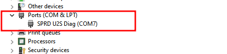
On a Linux machine, the USB port opens with VID 0x1782 and PID 0x4d00 values and on a Windows Machine, you should see the following COM port from the device manager.
Data Frame
The communication mechanism implemented by the protocol is a command/response mechanism that follows the following three steps:
- A command packet is sent to the device via
UART0. - The device processes and executes the command.
- A response packet is returned via the same channel.
A command and response packet is packed into the following data frame as the standard format:
7e [command|response pckt] [CRC-2] 7e
The data frame consists of 0x7e used to mark the start and end of the frame. Therefore, when this value is present in the body of the data frame (command, response or CRC) its escaped with 0x7d 0x5e and since 0x7d is used as an escaping parameter its also escaped with 0x7d 0x5d.
The CRC is a 2-byte value calculated against the command/response packet for detecting any bit errors during data transfer.
The process of packing a command packet into the data frame is as follows — this is performed when sending a response or when talking to the protocol:
- Construct the command packet.
- Calculate the CRC parity bit.
- Transcode or escape
0x7Eand0x7Dwith the values described above. - Add the header and tail to the data frame.
When the device receives the command — the data frame is unpacked as follows:
- The head and tail is removed from the packet.
- The escaped characters are decoded back to their previous values.
- A CRC check is performed and a response is returned.
CRC
This is the verification algorithm that is used to detect for any corruption during the serial communication. There are two CRC types:
- BROM-CRC: This is used when talking directly to the boot ROM.
- FDL-CRC: This is used when talking to the firmware downloaders — described in great detail below.
The following Python code snippet shows how these two variants can be calculated:
import binascii

def brom_crc(data: bytes): #used in boot mode
    crc = 0x0
    data = bytearray(data)
    _len = len(data)

    for ii in range(0, 1, 2):
        if ii + 1 == _len:
            crc += data[ii]
        else:
            crc += (data[ii] << 0x8) | data[ii + 0x1]

    crc = (crc >> 16) + (crc & 0xffff)
    crc += (crc >> 16)
    return ~crc & 0xffff

def fdl_crc(data: bytes): #used in FDL1/FDL2 mode
    return binascii.crc_hqx(data, 0)
Command & Response Packet
The command packet contains the instruction or the command to be executed by the device and any other additional data sent with the command. The following is a sample data frame that sends a Power Off command to the device.
[7e 00 17 00 00 ff e8 7e]
The breakdown of the above commands is as follows:
0x7e: This is obvious the head and tail of the data frame.00 17: This is theBSL_CMD_POWER_OFF|0x17command. A 2-byte value that instructs the device what to do.00 00: This is the data — since this command does not have any data (this value is NULL).ff e8: The CRC calculation performed against the command packet00 17 00 00
The following is a reponse received from the device in relation to the above command:
[7e 00 80 00 00 ff d7 7e]
The breakdown of the above response data frame is as follows:
00 80: This is theBSL_REP_ACK|0x80response to indicate command execution was a success.00 00: Since there is no data this value isNULLff d7: This is CRC value of the response packet.
The command and response packet signature skeleton is basically as follows:
7e [2-byte type] [data length] [data N-bytes] [CRC] 7e
For the above examples, the data was NULL. When writing a file to RAM, we need to include the following values to the command:
- Data Length: This is a 2-byte unsigned short and big endian value that specifies the length of the data included in the packet.
- Data: This is the actual data that can be included in a command or response. For example, the file being written to the device.
The list of supported commands and responses can be found in my github - here
Firmware Downloaders (FDL1/FDL2)
When the device is in BROM Mode, because of size limitations — the BROM code lives in a small space in the device’s ROM — not alot can be performed since it can’t handle complex tasks like formating partitions or intializing flash memory. The bootROM therefore expects a set of signed binary files called firmware downloaders.
These files are signed by the OEM using their own private keys — see the Android secure boot 8 to prevent execution of malicious files. There are two of these files, the first file FDL-1 is downloaded to the device’s RAM at a specific address and before execution, signature verification is performed by the boot ROM to check for the authenticity of the binary file.
The following is a sample data frame used to upload FDL-1 to RAM: [7e 00 01 00 08 00 00 50 00 00 00 cf d4 0c b1 7e]
- command:
BSL_CMD_START_DATA|0x1 - Data Length:
0x0008 - Data:
0x00005000+0x0000cfd4
The above command is preparing the Boot ROM to receive 0xcfd4 bytes of data in the RAM address 0x5000. These addresses are different and are based on the chip model. The next command uploads chunks of the executable each of size 0x210 because of the RAM’s limitations: [7e 00 02 02 10 41 41 41 41 ... 5c 5c 7e]
- command:
BSL_CMD_MIDST_DATA|0x2 - Data Length:
0x210 - Data:
0x414141..N - CRC:
0x5c5c
The above command uploads our binary to its address, the BSL_CMD_END_DATA|0x3 is used to indicate end of data transfer and now its ready for execution: [7e 00 04 00 00 dc c0 7e]
- command:
BSL_CMD_EXEC_DATA|0x4 - Data:
NULL
The above command executes the binary in its uploaded address. When the binary is executed and verified, BROM passes execution to it and it acts as the primary bootloader used to set memory requirements for the second file FDL-2. This executable is somewhat similar to EDL programmers in Qualcomm and the earlier mentioned Download Agents (DAs) in MTK devices.
NOTE:It is at this point that the CRC calculation changes since we are now communicating with a new preloader
A handshake is first sent to the preloader and this is a single 0x7e — this is a special command that does not follow the packet format and its used to check the baudrate. When the correct UART baudrate 115200 is correct on both side of the communication, FDL-1 responds with the following data Spreadtrum Boot Block Version on 1.1, this signals a successful connection and communication can now proceed from here.
Since the boot ROM and RAM limit download sizes, FDL-1 is downloaded first being smaller in size and FDL-2 follows. The main function of FDL-2 is to setup the flash memory of the device acting like the second bootloader.This can now allow for operations like writing to the flash memory and/or formatting partitions.
FDL-1 takes the same command as the boot ROM BSL_CMD_START_DATA|0x1 and BSL_CMD_MIDST_DATA|0x2 to prepare for the download of FDL-2 at a specific memory address. The following data frames describe this action.
[7e 00 01 00 08 9e ff fe 00 00 0f fa d4 68 12 7e]: This command prepares FDL-1 to receive 0xffad4 bytes of data in the memory address 0x9efffe00 — this address was specific to the DUT others might be different. This binary is also signed and therefore execution happens only after verification.
When FDL-2 is executed via BSL_CMD_EXEC_DATA|0x3 and context is switched to this preloader, the device responds with BSL_REP_INCOMPATIBLE_PARTITION|0x96 — this is a weird command for a response.This preloader can now accept commands like:
BSL_CMD_READ_FLASH|0x6: This command can be used to read partitions from the flash memory.BSL_CMD_ERASE_FLASH|0xA: This command takes an flash memory address to erase — used to erase partitions.BSL_CMD_READ_FLASH_INFO: A command used to get the flash size and block size.
The list of all other possible commands are provided in the resource mentioned earlier above. This here is a simple script written in Python that can be used to interact with a unisoc BROM.
Attack Surface
There is a wide attack surface in this area that can be a possible VR area for example memory corruption in the BROM code/preloaders and/or signature verification bypasses — CVE-2022-38694 is a classic example of an AAW that was discovered by the NCC group 8 that allows an attacker to overwrite a function pointer in the BootROM allowing for code execution with BROM priviledges.
Since the BROM code is read-only , the bug cannot be fixed via OTA making these bugs critical but only exploitable with physical access to the device. The above CVE has been used to bypass signature verification allowing attackers to load custom ROMs and root android devices. It has also be used by commercial flashing tools to bypass signature (FDL) verification providing custom loaders that are used for attacks like FRP Bypasses and the bypass of MDM solutions.
The next post will be the analysis of CVE-2022-38694 to create a POC that bypasses signature verification to write a custom OS to a vulnerable android device and also write our own firmware downloaders (FDLs).